
BSS84PWH6327XTSA1
Infineon BSS84PWH6327XTSA1 (small-signal MOSFET) is designed for high-voltage, high-current applications such as motor drives, power conversion and power amplification. Genuine original stock; Rds(on), Vceo and package thermal performance are per the official Datasheet. Contact us for pricing, samples and available stock.
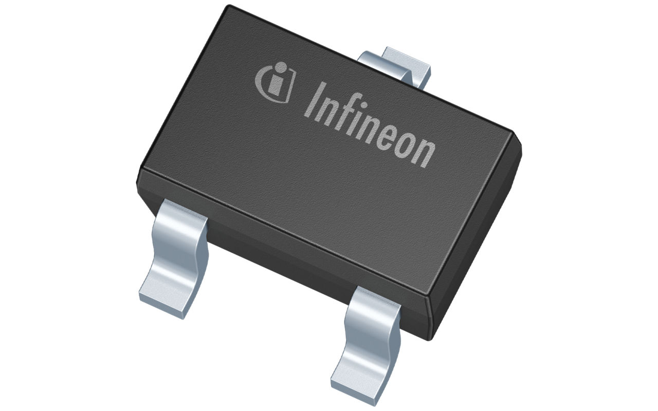
- Package
- SOT-323
Product overview
Infineon BSS84PWH6327XTSA1 (small-signal MOSFET) is designed for high-voltage, high-current applications such as motor drives, power conversion and power amplification. Genuine original stock; Rds(on), Vceo and package thermal performance are per the official Datasheet. Contact us for pricing, samples and available stock.
- Manufacturer
- Infineon
- Part number
- BSS84PWH6327XTSA1
- Category
- Small-Signal MOSFETs
- Package
- SOT-323
- Packaging
- Tape & Reel
- Condition
- New & Original
- Compliance
- RoHS Compliant
- Lifecycle
- Confirm with manufacturer
- Lead time / MOQ
- Confirm with quotation
Technical parameters
30 parametersConstruction
- Avalanche energy, single pulse
- 2.61 mJ
- Avalanche energy, periodic limited by Tjmax
- 0.03
- Reverse diode dv/dt dv/dt
- 6 kV/µs
- Power dissipation Ptot
- 0.3 W
- Rev 2.0 Page 1
- 2016-06- 21
- VDS = -60 V, V GS = 0 V, T j = 25 °C
- 0.1
- VDS = -60 V, V GS = 0 V, T j = 125 °C
- 10
- Rev 2.0 Page 2
- 2016-0 6-21
- Transconductance g fs V DS£2*ID*R DS(on)max , 0.08
- 0.16 S
- Input capacitance Ciss V GS=0V, VDS=-25V
- 15.3 pF
- Output capacitance Coss f=1MHz
- 5.8
- Reverse transfer capacitance Crss
- 3
- Turn-on delay time t d(on) V DD=-30V, V GS=-4.5V
- 6.7 ns
- Rise time tr ID=-0.12A, RG=25W
- 16.2
- Turn-off delay time t d(off)
- 8.6
- Fall time tf
- 20.5
- Gate to source charge Q gs V DD=-48V, I D=-0.15A
- 0.25 nC
- Gate to drain charge Q gd
- 0.3
- Gate charge total Qg V DD=-48V, I D=-0.15A
- 1
- Reverse recovery time t rr V R=-30V, I F=l S
- 23.6 ns
- Reverse recovery charge Q rr diF/dt=100A/µs
- 11.6 nC
- Rev 2.0 Page 3
- 2016-06- 21
Performance
- Continuous drain current
- 0.15 A
- Gate source voltage
- ±20 V
- Operating and storage temperature Tj , Tstg -5
- 5...+150 °C
- Gate threshold voltage, VGS = VDS VGS(th) -1
- 1.5
- Gate-source leakage current IGSS
- 10 nA
- Drain-source on-state resistance RDS(on)
- 10.5 W
- Gate plateau voltage V(plateau) V DD=-48V, ID=-0.15A
- 3.4 V
- Inverse diode forward voltage VSD V GS=0V, IF=-0.15A
- 0.84
Specifications & documentation
Use the official manufacturer documentation to verify electrical characteristics, package dimensions and operating limits before design approval.
Frequently asked questions
Common pre-quotation questions and selection notes to help you verify key parameters and sourcing before requesting a quote.
What is a drop-in replacement for BSS84PWH6327XTSA1?
BSS84PWH6327XTSA1 is an N-channel 1.5 / 0.15 A MOSFET in SOT-323. A pin-to-pin compatible substitute must match three things: V_DS ≥ 1.5, R_DS(on) ≤ 10.5 W, and the identical SOT-323 footprint. Always verify avalanche rating and gate charge (Q_g ≈ 1) against your driver before swapping.
How do I choose a MOSFET alternative?
Three checks: (1) V_DS must be ≥ original with ~20% headroom for spikes; (2) R_DS(on) should be ≤ original, evaluated at your real operating temperature; (3) package must be identical (TO-220 ≠ TO-263). Also confirm gate charge (Q_g) and avalanche energy match, or re-test the driver.
Which parameters matter most when comparing MOSFETs?
Focus on V_DS (voltage rating), I_D (continuous current at your case temperature, not just 25 °C), R_DS(on) (conduction loss), and Q_g (switching speed / driver match). For inductive loads, also check avalanche rating.
How do I verify the part is genuine / avoid counterfeit?
Buy only from authorized or franchised channels. On receipt, check: (1) laser-etched markings that solvent will not remove; (2) batch / lot code consistent between label and device; (3) original reel or tube packaging; (4) request traceability documents (CoC, date code). For critical parts, third-party X-ray / decapsulation testing is recommended.
How do I read the markings / date code on a chip?
Most active ICs use a 4-digit date code YYWW (year + week, e.g. 2345 = 2023 week 45). The top mark is manufacturer logo + base part number + lot code. For SMD code lookup, search by "marking code + package" on AllDataSheet / Octopart / LCSC.
What does the package code mean (TO-220, SOT-23, QFP…)?
Package codes describe the physical form factor and pin layout — critical when sourcing, because electrically equivalent parts in different packages will not fit the PCB. Common: TO-220 (3-terminal power), SOT-23 (3-pin small signal), DIP / SOIC (through-hole / SMD ICs), QFP / QFN (MCUs, processors).
What if my original model is discontinued (EOL / NRND)?
Three options: (1) the manufacturer’s recommended replacement; (2) franchised distributor legacy stock; (3) a functionally compatible cross-brand part — provided pinout and key parameters match. Always evaluate on a real board before mass swap.
What is the minimum order quantity (MOQ) and lead time?
We support both sample and volume orders. Minimum order quantity, stock availability and lead time are confirmed per inquiry — tell us your model and quantity and we will quote. Sample quantities for design validation are supported.
Can I get the datasheet and samples?
The full datasheet is linked on this page. For parts without a direct datasheet, we can locate the manufacturer document on request. Sample requests are supported — contact us with your model and quantity.
Request confirmation of current stock, date code, packaging, price and delivery terms. Product information does not constitute a binding offer; final specifications are confirmed with your quotation.