
TPS61086DRCR
The TPS61086 is a high-frequency step-up converter that generates outputs up to 18.5 V from a 2.3-V to 6-V input, using a 2-MHz fixed switching frequency and a 2.6-A typical switch-current limit. It features an enable pin, power-good indicator and light-load efficiency mode, with 70-nA typical quiescent current. It is suited to bias supplies for displays, sensors and power amplifiers in portable and industrial systems.
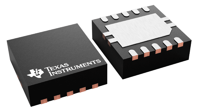
- Package
- VSON-10
Product overview
The TPS61086 is a high-frequency step-up converter that generates outputs up to 18.5 V from a 2.3-V to 6-V input, using a 2-MHz fixed switching frequency and a 2.6-A typical switch-current limit. It features an enable pin, power-good indicator and light-load efficiency mode, with 70-nA typical quiescent current. It is suited to bias supplies for displays, sensors and power amplifiers in portable and industrial systems.
- Manufacturer
- TI
- Part number
- TPS61086DRCR
- Category
- Power Management
- Package
- VSON-10
- Packaging
- Tape & Reel
- Condition
- New & Original
- Compliance
- RoHS Compliant
- Lifecycle
- Confirm with manufacturer
- Lead time / MOQ
- Confirm with quotation
Technical parameters
31 parametersConstruction
- Human body model (HBM), per ANSI/ESDA/JEDEC JS-001
- ±2000
- Machine Model
- ±200
- TSDHYS Thermal shutdown hysteresis
- 14
- gm Transconductance error amplifier
- 107
- fS Oscillator frequency
- 0.9
- VIN rising
- 2.3 V
- Line regulation VIN = 2.3 V to 6 V, IOUT = 10 mA
- 0002 %/V
- Load regulation VIN = 3.3 V, IOUT = 1 mA to 400
- 0.11
Performance
- Input voltage IN
- 7 V
- Voltage on pins EN, FB, SS, MODE
- 7 V
- Voltage on pin
- 20 V
- Operating junction temperature
- 150 °C
- Storage temperature
- 150 °C
- VIN Input voltage
- 6 V
- VS Boost output voltage VIN +
- 18.5 V
- TA Operating free-air temperature
- 85 °C
- TJ Operating junction temperature
- 125 °C
- VIN Input voltage range
- 2.3
- VFB Feedback regulation voltage
- 1.23
- ILIM N-channel MOSFET current limit
- 2
- ISDVIN Shutdown current into IN EN =
- 1 μA
- VUVLO Undervoltage lockout threshold VIN falling
- 2.2 V
- TSD Thermal shutdown Temperature rising
- 150 °C
- VIH High level input voltage VIN = 2.3 V to 6
- 2 V
- VIL Low level input voltage VIN = 2.3 V to 6
- 0.5 V
- IINLEAK Input leakage current EN =
- 0.1 μA
- VS Boost output voltage
- 18.5 V
- IFB Feedback input bias current VFB = 1.238
- 0.1 μA
- VIN = VGS = 3.3 V, ISW = current
- 0.16
- ISWLEAK SW leakage current EN = GND, VSW = 6
- 10 μA
- ISS Soft-start current VSS = 1.238
- 10 μA
Specifications & documentation
Use the official manufacturer documentation to verify electrical characteristics, package dimensions and operating limits before design approval.
Request confirmation of current stock, date code, packaging, price and delivery terms. Product information does not constitute a binding offer; final specifications are confirmed with your quotation.