
TPS54302DDCR
The TPS54302 is a 3-A synchronous step-down converter operating from a 4.5 V to 28 V input with adjustable output down to 0.6 V. It uses current-mode control with spread-spectrum EMI reduction, 40 uA quiescent current, fixed soft-start and adjustable UVLO. Rated -40 degC to 125 degC, it targets industrial, consumer and wide-VIN power supplies.
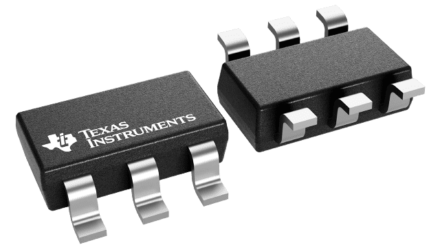
- Package
- SOT-23-THN-6
Product overview
The TPS54302 is a 3-A synchronous step-down converter operating from a 4.5 V to 28 V input with adjustable output down to 0.6 V. It uses current-mode control with spread-spectrum EMI reduction, 40 uA quiescent current, fixed soft-start and adjustable UVLO. Rated -40 degC to 125 degC, it targets industrial, consumer and wide-VIN power supplies.
- Manufacturer
- TI
- Part number
- TPS54302DDCR
- Category
- Power Management
- Package
- SOT-23-THN-6
- Packaging
- Tape & Reel
- Condition
- New & Original
- Compliance
- RoHS & REACH Compliant
- Lifecycle
- Confirm with manufacturer
- Lead time / MOQ
- Confirm with quotation
Technical parameters
32 parametersConstruction
- VIN
- = 12 V
- FB
- 7 V
- BOOT-SW
- 7 V
- SW (20ns transient)
- 30 V
- SW
- 28 V
- Rising
- 4.1 V
- VIN(UVLO) Falling
- 3.6 V
- Hysteresis
- 480 mV
- VENrising Rising
- 1.23 V
- VENfalling Falling
- 1.16 V
- fSW Centre switching f
- 290
- Hiccup time
- 32768
- fSW Centre switching frequen
- 290
- tHIC_WAIT Hiccup wait time
- 512 es
- tHIC_RESTART Hiccup time before restart
- 6384 es
- tSS Soft-start time
- 5 ms
- tMIN_ON
- 110 ns
Performance
- Input voltage, VI
- 7 V
- Output voltage, VO
- 30 V
- Operating junction temperature
- 150 °C
- Storage temperature, Tstg
- 150 °C
- VI Input voltage
- 5.5 V
- TJ Operating junction temperature
- 125 °C
- VIN Input voltage range
- 28 V
- IQ Non switching quiescent current EN = 5V, VFB = 1V
- 45 µA
- IOFF Shut down current EN =
- 2 µA
- I(EN_INPUT) Input current VEN = 1V
- 0.7 μA
- I(EN_HYS) Hysteresis current VEN = 1.5V
- 1.55 μA
- VFB Feedback Voltage VIN = 12V 0
- 0.611 V
- R(HSD) High-side FET on resistance TA = 25°C, VBST – SW = 5V
- 85 mΩ
- R(LSD) Low-side FET on resistance TA = 25°C, VIN = 12V
- 40 mΩ
- Rising temperature
- 160
Specifications & documentation
Use the official manufacturer documentation to verify electrical characteristics, package dimensions and operating limits before design approval.
Request confirmation of current stock, date code, packaging, price and delivery terms. Product information does not constitute a binding offer; final specifications are confirmed with your quotation.