
TLV320AIC3212IYZFR
The TLV320AIC3212 is a low-power stereo audio CODEC integrating two ADC channels and two DAC channels with 93-dB ADC and 100-dB DAC SNR and up to 192-kHz sampling. It includes a stereo Class-D speaker amplifier, a stereo headphone amplifier and a receiver/earpiece driver, with I2S/PCM/TDM digital and I2C/SPI control interfaces and 8 analog inputs and 7 analog outputs. It targets smartphones, tablets and portable media devices requiring compact, battery-efficient audio.
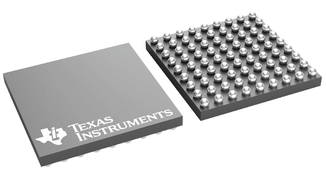
- Package
- DSBGA-81
Product overview
The TLV320AIC3212 is a low-power stereo audio CODEC integrating two ADC channels and two DAC channels with 93-dB ADC and 100-dB DAC SNR and up to 192-kHz sampling. It includes a stereo Class-D speaker amplifier, a stereo headphone amplifier and a receiver/earpiece driver, with I2S/PCM/TDM digital and I2C/SPI control interfaces and 8 analog inputs and 7 analog outputs. It targets smartphones, tablets and portable media devices requiring compact, battery-efficient audio.
- Manufacturer
- TI
- Part number
- TLV320AIC3212IYZFR
- Category
- Audio
- Package
- DSBGA-81
- Packaging
- Tape & Reel
- Condition
- New & Original
- Compliance
- RoHS Compliant
- Lifecycle
- Confirm with manufacturer
- Lead time / MOQ
- Confirm with quotation
Technical parameters
39 parametersConstruction
- AVDD1_18, AVDD2_18, AVDD4_18, AVDD_18 to AVSS1, AVSS2, AVSS4
- 2.2 V
- AVDD3_33 to AVSS3 and RECVDD_33 to
- 3.9 V
- DVDD to
- 2.2 V
- IOVDD to
- 3.9 V
- HVDD_18 to
- 2.2 V
- CPVDD_18 to
- 2.2 V
- SLVDD to SLVSS, SRVDD to SRVSS, SPK_V to SRVSS
- 6 V
- VBAT
- 6 V
- Human-body model (HBM), per ANSI/ESDA/JEDEC JS-001
- ±2400
- respectively (1) TI recommends connecting each of
- 1.8
- Referenced to AVSS3 and RECVSS respectively 1.6
- 3.3
- IOVDD Referenced to IOVSS
- 3.6
- CF Type
- 2.2 µF
- Input impedance IN1L/AUX1 or IN1R/AUX2 Selected
- 1 ÷ (f×CSAR_IN kΩ
- Input capacitance
- 25 pF
- Input signal level (0dB) Single-ended, CM = 0.9
- 0.5 VRMS
- Inputs AC-shorted to ground
- 93
- weighted (1)
- 93
- DR –60dB full-scale, 1-kHz input signal
- 93 dB
- 3 dB full-scale, 1-kHz input signal
- 87
- Gain Error
- 0.1 dB
- IN1L routed to Left ADC, IN1R routed to Right ADC, Rin = 20
- 110 dB
- Input Pin Crosstalk routed
- 116 dB
- DR –60-dB full-scale, 1-kHz input signal
- 91 dB
- THD+N –3-dB full-scale, 1-kHz input signal
- 85 dB
- SNR Inputs AC-shorted to ground
- 94 dB
- THD+N –3dB full-scale, 1-kHz input signal
- 88 dB
- Input Pin Crosstalk internally not routed
- 109 dB
- PSRR
- 59 dB
- IN1 - IN3, Single-Ended, Rin = 10 K, PGA gain set to 0 dB
- 0 dB
- IN1 - IN3, Single-Ended, Rin = 10 K, PGA gain set to 47.5 dB
- 47.5 dB
- IN1 - IN3, Single-Ended, Rin = 20 K, PGA gain set to 0 dB
- 6 dB
- IN1 - IN3, Single-Ended, Rin = 40 K, PGA gain set to 47.5 dB
- 35.5 dB
Performance
- Analog input voltage to ground
- 18 + 0.3 V
- Operating temperature
- 85 °C
- Junction temperature (TJ Max)
- 105 °C
- Storage temperature
- 125 °C
- TOPR Operating temperature range
- 85 °C
- Input leakage current
- 1 µA
Specifications & documentation
Use the official manufacturer documentation to verify electrical characteristics, package dimensions and operating limits before design approval.
Request confirmation of current stock, date code, packaging, price and delivery terms. Product information does not constitute a binding offer; final specifications are confirmed with your quotation.