
SN74AHCT1G08DBVR
The SN74AHCT1G08 is a single 2-input positive-AND gate in the AHCT logic family with TTL-compatible CMOS inputs and push-pull outputs. It operates from 4.5V to 5.5V, supports data rates up to 70Mbps, and offers sub-10ns propagation delay. It is used for basic logic gating and 5V level translation.
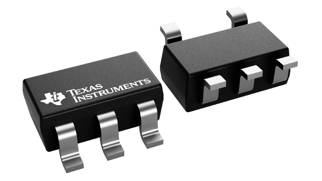
- Package
- SOT-23-5 (DBV)
Product overview
The SN74AHCT1G08 is a single 2-input positive-AND gate in the AHCT logic family with TTL-compatible CMOS inputs and push-pull outputs. It operates from 4.5V to 5.5V, supports data rates up to 70Mbps, and offers sub-10ns propagation delay. It is used for basic logic gating and 5V level translation.
- Manufacturer
- TI
- Part number
- SN74AHCT1G08DBVR
- Category
- Logic
- Package
- SOT-23-5 (DBV)
- Packaging
- Tape & Reel
- Condition
- New & Original
- Compliance
- RoHS Compliant
- Lifecycle
- Confirm with manufacturer
- Lead time / MOQ
- Confirm with quotation
Technical parameters
34 parametersConstruction
- Human-body model (HBM), per ANSI/ESDA/JEDEC JS-001
- ±2500
- Δt/Δv Input transition rise and fall rate
- 20 ns/V
- High-level output TA = –40°C to 125°C
- 4.4
- IOL = 50 µA, VCC = 4.5
- 0.1
- VOL TA = 25°C
- 0.36 V
- VI = 5.5 V or GND, TA = 25°C
- ±0.1
- VCC = 0 V to 5.5 V TA = –40°C to 125°C
- ±1
- VI = VCC or GND, IO = 0, TA = 25°C
- 1
- VCC = 5.5 V TA = –40°C to 125°C
- 10
- Change in supply One input at 3.4 V, Other Inputs TA = 25°C
- 1.35
- CI Input capacitance VI = VCC or GND, VCC = 5
- 4 pF
- tPLH A or B Y CL = 15 pF TA = –40°C to 85°C
- 7.1 ns
- tPHL A or B Y CL = 15 pF TA = –40°C to 85°C
- 7.1 ns
- tPLH A or B Y CL = 50 pF
- 9 ns
- tPHL A or B Y CL = 50 pF TA = –40°C to 85°C
- 9 ns
- Cpd Power dissipation capacitance No load, f = 1 MHz
- 18 pF
Performance
- VCC Supply voltage
- 5.5 V
- VI Input voltage(2)
- 7 V
- VO Output voltage(2)
- 0.5 V
- IIK Input clamp current VI < 0
- 20 mA
- IOK Output clamp current VO < 0 or VO >
- ±20 mA
- IO Continuous output current VO = 0 to
- ±25 mA
- Continuous current through VCC or
- ±50 mA
- TJ Maximum junction temperature
- 150 °C
- Tstg Storage temperature
- 150 °C
- VIH High-level input voltage
- 2 V
- VIL Low-level input voltage
- 0.8 V
- VI Input voltage
- 5.5 V
- VO Output voltage
- 0 V
- IOH High-level output current
- 8 mA
- IOL Low-level output current
- 8 mA
- TA Operating free-air temperature
- 125 °C
- voltage TA = 25°C
- 3.94
- current at VCC or GND, VCC = 5.5 V TA = –40°C to 125°C
- 1.5
Specifications & documentation
Use the official manufacturer documentation to verify electrical characteristics, package dimensions and operating limits before design approval.
Request confirmation of current stock, date code, packaging, price and delivery terms. Product information does not constitute a binding offer; final specifications are confirmed with your quotation.