
SN74ACT574PWR
The SN74ACT574 contains eight D-type edge-triggered flip-flops with 3-state outputs, a 90-MHz maximum clock frequency, and TTL-compatible CMOS inputs. It supports 24-mA output drive and operates from -40 C to 85 C. It is used for buffered data storage and bus interfacing in logic systems.
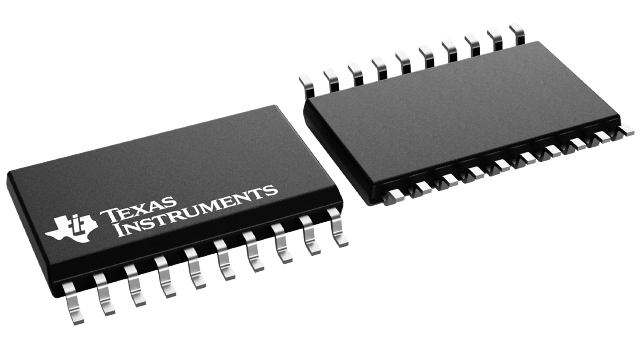
- Package
- TSSOP-20
Product overview
The SN74ACT574 contains eight D-type edge-triggered flip-flops with 3-state outputs, a 90-MHz maximum clock frequency, and TTL-compatible CMOS inputs. It supports 24-mA output drive and operates from -40 C to 85 C. It is used for buffered data storage and bus interfacing in logic systems.
- Manufacturer
- TI
- Part number
- SN74ACT574PWR
- Category
- Logic
- Package
- TSSOP-20
- Packaging
- Tape & Reel
- Condition
- New & Original
- Compliance
- RoHS & REACH Compliant
- Lifecycle
- Confirm with manufacturer
- Lead time / MOQ
- Confirm with quotation
Technical parameters
11 parametersConstruction
- Human-body model (HBM), per ANSI/ESDA/JEDEC JS-001
- ±2000
- Charged-device model (CDM), per ANSI/ESDA/JEDEC JS-002
- ±1000
- Cpd Power dissipation capacitance CL = 50 pF, f = 1 MHz
- 40 pF
Performance
- VCC Supply voltage range
- 7 V
- VI Input voltage range
- −0.5 V
- VO Output voltage range
- −0.5 V
- IIK Input clamp current (VI < 0 or VI > VCC)
- ±20 mA
- IOK Output clamp current (VO < 0 or VO > VCC)
- ±20 mA
- IO Continuous output current (VO = 0 to VCC)
- ±50 mA
- Continuous current through VCC or
- ±200 mA
- Tstg Storage temperature range
- 150 °C
Specifications & documentation
Use the official manufacturer documentation to verify electrical characteristics, package dimensions and operating limits before design approval.
Request confirmation of current stock, date code, packaging, price and delivery terms. Product information does not constitute a binding offer; final specifications are confirmed with your quotation.