
LP5907MFX-3.3/NOPB
The LP5907 is a 250mA LDO with 6.5uVRMS output noise, 60dB PSRR at 100kHz, and a 120mV typical dropout voltage. It operates from 2.2V to 5.5V with a 12uA typical quiescent current and includes enable and output discharge functions. It is designed to power noise-sensitive RF and analog loads.
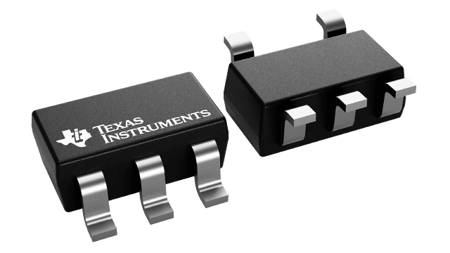
- Package
- SOT-23-5 (DBV)
Product overview
The LP5907 is a 250mA LDO with 6.5uVRMS output noise, 60dB PSRR at 100kHz, and a 120mV typical dropout voltage. It operates from 2.2V to 5.5V with a 12uA typical quiescent current and includes enable and output discharge functions. It is designed to power noise-sensitive RF and analog loads.
- Manufacturer
- TI
- Part number
- LP5907MFX-3.3/NOPB
- Category
- Power Management
- Package
- SOT-23-5 (DBV)
- Packaging
- Tape & Reel
- Condition
- New & Original
- Compliance
- RoHS Compliant
- Lifecycle
- Confirm with manufacturer
- Lead time / MOQ
- Confirm with quotation
Technical parameters
43 parametersConstruction
- Human-body model (HBM), per ANSI/ESDA/JEDEC JS-001
- ±2000
- IOUT = 1mA to 250mA
- 3
- Line regulation
- 0.02 %/V
- Load regulation IOUT = 1mA to 250mA
- 0 %/mA
- VEN = 1.2V, IOUT = 0mA
- 12
- VEN = 0.3V (disabled)
- 0.2
- IOUT = 100mA
- 50
- IOUT = 250mA (SOT-23, X2SON packages)
- 250
- f = 100Hz, IOUT = 20mA
- 90
- f = 1kHz, IOUT = 20mA
- 82
- f = 10kHz, IOUT = 20mA
- 65
- f = 100kHz, IOUT = 20mA
- 60
- IOUT = 1mA
- 10
- IOUT = 250mA
- 6.5
- RAD VEN < VIL (output disabled)
- 230 Ω
- Thermal shutdown TJ rising
- 160
- Thermal hysteresis TJ falling from shutdown
- 15
- VIL Low input threshold
- 0.4 V
- VIH High input threshold
- 1.2 V
- VEN = 5.5V and VIN = 5.5V
- 5.5
- VEN = 0V and VIN = 5.5V
- 0
- IOUT = 1mA to 250mA in 10µs
- 40
- ΔVOUT IOUT = 250mA to 1mA in 10µs
- 40
- Overshoot on start-up(9) Stated as a percentage of VOUT(NOM)
- 5%
- Overshoot on start-up with EN
- 1%
- tON Turn-on time
- 80 µs
- CIN Input capacitance(2) 0.7
- 1 µF
Performance
- VIN Input voltage
- 6 V
- VOUT Output voltage
- 0.3 V
- VEN Enable input voltage
- 5.5 V
- TJMAX Junction temperature
- 150 °C
- Tstg Storage temperature
- 150 °C
- VIN Input supply voltage
- 5.5 V
- IOUT Output current
- 250 mA
- TJ Junction temperature
- 125 °C
- TA Ambient temperature
- 85 °C
- VIN Input voltage TA = 25°C
- 5.5 V
- Load current See
- 250 mA
- Maximum output current
- 250 mA
- IQ Quiescent current(5) VEN = 1.2V, IOUT = 250mA
- 250 μA
- IG Ground current(6) VEN = 1.2V, IOUT = 0mA
- 14 μA
- VDO Dropout voltage(7) IOUT = 250mA (DSBGA package)
- 120 mV
- ISC Short-circuit current limit TA = 25°C
- 500 mA
Specifications & documentation
Use the official manufacturer documentation to verify electrical characteristics, package dimensions and operating limits before design approval.
Request confirmation of current stock, date code, packaging, price and delivery terms. Product information does not constitute a binding offer; final specifications are confirmed with your quotation.