
LMV358IDGKR
The LMV358 is a low-voltage dual operational amplifier with a 2.7-V to 5.5-V supply range, 1-MHz gain-bandwidth product, 1 V/us slew rate and rail-to-rail output stage. It offers 7 mV maximum offset, 0.105 mA typical quiescent current per channel and bipolar input common-mode extending below the negative rail. Typical uses include portable and battery-powered consumer and industrial equipment, sensor buffering and low-side current sensing.
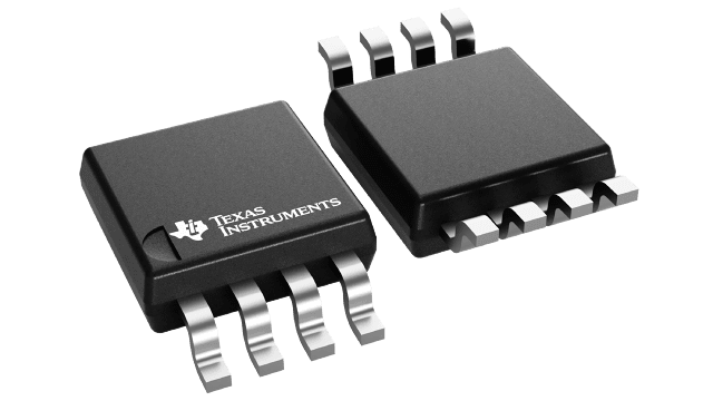
- Package
- VSSOP-8
Product overview
The LMV358 is a low-voltage dual operational amplifier with a 2.7-V to 5.5-V supply range, 1-MHz gain-bandwidth product, 1 V/us slew rate and rail-to-rail output stage. It offers 7 mV maximum offset, 0.105 mA typical quiescent current per channel and bipolar input common-mode extending below the negative rail. Typical uses include portable and battery-powered consumer and industrial equipment, sensor buffering and low-side current sensing.
- Manufacturer
- TI
- Part number
- LMV358IDGKR
- Category
- Amplifiers & Linear
- Package
- VSSOP-8
- Packaging
- Tape & Reel
- Condition
- New & Original
- Compliance
- RoHS Compliant
- Lifecycle
- Confirm with manufacturer
- Lead time / MOQ
- Confirm with quotation
Technical parameters
39 parametersConstruction
- Human-body model (HBM), per ANSI/ESDA/JEDEC JS-001
- ±2000
- Vs = 5
- ±1
- Vs = 5 V, TA = –40°C to 125°C
- ±5
- VCM No phase reversal, rail-to-rail input (V–)
- 0.1 V
- En ƒ = 0.1 Hz to 10 Hz, Vs = 5
- 5.1 µVPP
- ƒ = 1 kHz, Vs = 5
- 33
- ƒ = 10 kHz, Vs = 5
- 30
- CID Differential
- 1.5 pF
- CIC Common-mode
- 5 pF
- VS = 5.5 V, (V–) + 0.05 V < VO < (V+) – 0.05 V, RL = 10 kΩ
- 115
- VS = 2.5 V, (V–) + 0.04 V < VO < (V+) – 0.04 V, RL = 10 kΩ
- 98
- VS = 2.5 V, (V–) + 0.1 V < VO < (V+) – 0.1 V, RL = 2 kΩ
- 112
- VS = 5.5 V, (V–) + 0.15 V < VO < (V+) – 0.15 V, RL = 2 kΩ
- 128
- GBW Gain-bandwidth product Vs = 5
- 1 MHz
- φm Phase margin VS = 5.5 V, G = 1
- 76 °
- SR Slew rate Vs = 5
- 1.7 V/µs
- To 0.1%, VS = 5 V, 2-V step , G = +1, CL = 100 pF
- 3
- To 0.01%, VS = 5 V, 2-V step , G = +1, CL = 100 pF
- 4
- tOR Overload recovery time VS = 5 V, VIN × gain >
- 0.9 µs
- THD+N
- 005%
- from supply rails VS = 5.5 V, RL = 2 kΩ
- 40
- ZO Open-loop output impedance Vs = 5 V, f = 1 MHz
- 1200 Ω
- IO = 0 mA, VS = 5.5
- 70
- IO = 0 mA, VS = 5.5 V, TA = –40°C to 125°C
- 150
- Power-on time VS = 0 V to 5 V, to 90% IQ level
- 50 µs
Performance
- Supply voltage, ([V+] – [V–])
- 6 V
- Current
- 10 mA
- Operating
- 150 °C
- Operating junction temperature
- 150 °C
- Storage temperature, Tstg
- 150 °C
- VS Supply voltage
- 5.5 V
- TA Specified temperature
- 125 °C
- dVOS/dT VOS vs temperature TA = –40°C to 125°C
- ±1 V/°C
- IB Input bias current Vs = 5
- ±10 pA
- IOS Input offset current
- ±3 pA
- in Input current noise density ƒ = 1 kHz, Vs = 5
- 25 A/√Hz
- Voltage output swing VS = 5.5 V, RL = 10 kΩ
- 20
- ISC Short-circuit current Vs = 5.5
- ±40 mA
- VS Specified voltage range 2.5 (±
- 5.5 ( V
Specifications & documentation
Use the official manufacturer documentation to verify electrical characteristics, package dimensions and operating limits before design approval.
Request confirmation of current stock, date code, packaging, price and delivery terms. Product information does not constitute a binding offer; final specifications are confirmed with your quotation.