
INA199B2QDCKRQ1
The INA199-Q1 is an AEC-Q100 qualified, bidirectional current-sense amplifier that measures voltage across a shunt resistor on either the high or low side. It offers fixed gains of 50, 100 or 200 V/V, a maximum input offset of 150uV, a common-mode range of -0.3V to 26V, and a bandwidth up to 80kHz. The B2 version provides a gain of 100 V/V and operates from -40C to 125C.
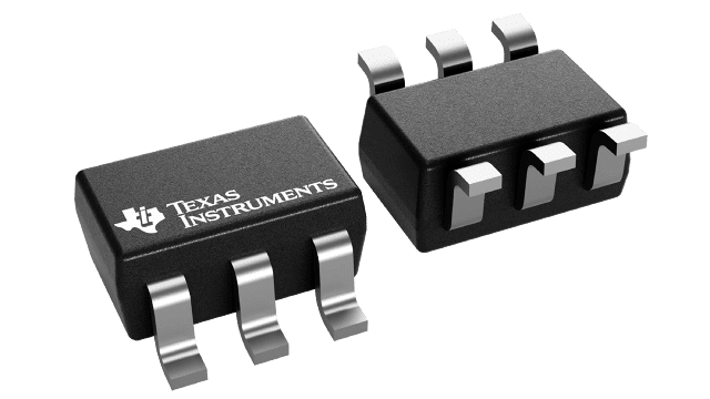
- Package
- SOT-SC70-6
Product overview
The INA199-Q1 is an AEC-Q100 qualified, bidirectional current-sense amplifier that measures voltage across a shunt resistor on either the high or low side. It offers fixed gains of 50, 100 or 200 V/V, a maximum input offset of 150uV, a common-mode range of -0.3V to 26V, and a bandwidth up to 80kHz. The B2 version provides a gain of 100 V/V and operates from -40C to 125C.
- Manufacturer
- TI
- Part number
- INA199B2QDCKRQ1
- Category
- Amplifiers & Linear
- Package
- SOT-SC70-6
- Packaging
- Tape & Reel
- Condition
- New & Original
- Compliance
- RoHS & REACH Compliant
- Lifecycle
- Confirm with manufacturer
- Lead time / MOQ
- Confirm with quotation
Technical parameters
28 parametersConstruction
- Differential (VIN+) – (VIN–)
- 26
- Analog inputs, VIN+, VIN– (2) Common-mode(3), INA199Ax
- 26 V
- Common-mode(3), INA199Bx and INA199Cx
- 26
- REF input
- 0.3 V
- Output
- 0.3 V
- Human-body model (HBM), per ANSI/ESDA/JEDEC JS-001
- ±2000
- Version A, TA = –40°C to 125°C
- 26
- Version B and C, TA = –40°C to 125°C
- 26
- CMR Common-mode rejection
- 120 dB
- PSR Power supply rejection
- ±0.1 μV/V
- INA199x1
- 50
- G Gain INA199x2
- 100 V/V
- INA199x3
- 200
- Nonlinearity error VSENSE = –5 mV to 5 mV
- 01%
- Maximum capacitive load No sustained oscillation
- 1 nF
Performance
- Supply voltage
- 26 V
- Input current Into all pins
- 5 mA
- Operating temperature
- 125 °C
- Junction temperature
- 150 °C
- Storage temperature, Tstg
- 150 °C
- VCM Common-mode input voltage
- 12 V
- VS Operating supply voltage (applied to V+)
- 5 V
- TA Operating free-air temperature
- 125 °C
- VOS Offset voltage, RTI(1) VSENSE = 0 mV
- ±5 μV
- dVOS/dT VOS vs temperature TA = –40°C to 125°C
- 0.1 μV/°C
- IB Input bias current VSENSE = 0 mV
- 28 μA
- IOS Input offset current VSENSE = 0 mV
- 0.02 μA
- Gain error vs temperature TA = –40°C to 125°C
- 3 /°C
Specifications & documentation
Use the official manufacturer documentation to verify electrical characteristics, package dimensions and operating limits before design approval.
Request confirmation of current stock, date code, packaging, price and delivery terms. Product information does not constitute a binding offer; final specifications are confirmed with your quotation.