
DAC8811IBDGKR
The DAC8811 is a 16-bit serial-input (SPI) multiplying digital-to-analog converter with an unbuffered current output, +/-1 LSB INL and a 0.5 us settling time. It uses an external reference, consumes only 0.025 mW typical, and operates from -40 to 105 C at up to 2 MSPS. It is suited to precision waveform generation, automatic test equipment and instrumentation.
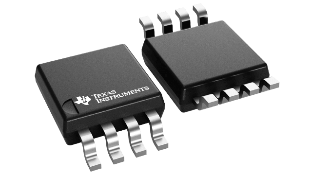
- Package
- VSSOP-8
Product overview
The DAC8811 is a 16-bit serial-input (SPI) multiplying digital-to-analog converter with an unbuffered current output, +/-1 LSB INL and a 0.5 us settling time. It uses an external reference, consumes only 0.025 mW typical, and operates from -40 to 105 C at up to 2 MSPS. It is suited to precision waveform generation, automatic test equipment and instrumentation.
- Manufacturer
- TI
- Part number
- DAC8811IBDGKR
- Category
- Data Converters
- Package
- VSSOP-8
- Packaging
- Tape & Reel
- Condition
- New & Original
- Compliance
- RoHS & REACH Compliant
- Lifecycle
- Confirm with manufacturer
- Lead time / MOQ
- Confirm with quotation
Technical parameters
38 parametersConstruction
- VDD to
- 7 V
- V (IOUT) to
- 0.3 V
- Human body model (HBM), per ANSI/ESDA/JEDEC JS-001
- ±4000
- Resolution
- 16 Bits
- Relative accuracy DAC8811C
- ±1 LSB
- Relative accuracy DAC8811B
- ±2 LSB
- Differential nonlinearity
- ±0.5 LSB
- Full-scale gain error All ones loaded to DAC register
- ±1 mV
- Full-scale tempco
- ±3 pm/°C
- Output capacitance Code dependent
- 50 pF
- VREF Range
- 15 V
- Input capacitance
- 5 pF
- VDD = 2.7V
- 0.6 V
- VDD = 5V
- 0.8 V
- CIL Input capacitance
- 10 pF
- VDD
- 5.5 V
- IDD (normal operation) Logic inputs = 0
- 5 µA
- VDD = 4.5 V to 5.5 V VIH = VDD and VIL =
- 3 µA
- VDD = 2.7 V to 3.6 V VIH = VDD and VIL =
- 1 µA
- fCLK Clock input frequency
- 50 MHz
- t(CH) Clock pulse width high
- 10 ns
- t(CL) Clock pulse width low
- 10 ns
- t(CSS) CS to Clock setup time
- 0 ns
- t(CSH) Clock to CS hold time
- 10 ns
- t(DS) Data setup time
- 5 ns
- t(DH) Data hold time
- 10 ns
Performance
- Digital input voltage
- 0.3 V
- Reference voltage, VREF RFB to
- 25 V
- Operating temperature
- 105 °C
- Junction temperature
- 125 °C
- Storage temperature, Tstg
- 150
- Supply voltage to
- 5.5 V
- Operating ambient temperature
- 125 °C
- Output leakage current Data = 0000h, TA = 25°C
- 10 nA
- Output leakage current Data = 0000h, TA =
- 10 nA
- Output current
- 2 mA
- Input resistance
- 5 kΩ
- IIL Input leakage current
- 10 µA
Specifications & documentation
Use the official manufacturer documentation to verify electrical characteristics, package dimensions and operating limits before design approval.
Request confirmation of current stock, date code, packaging, price and delivery terms. Product information does not constitute a binding offer; final specifications are confirmed with your quotation.