
BQ294704DSGT
The BQ2947 is a second-level overvoltage protector for 2-, 3- or 4-series cell Li-ion battery packs, monitoring each cell and triggering an external FET off-state when any cell exceeds its overvoltage threshold (selectable from 4.125 V to 4.6 V). It uses a single-pin output drive with an external delay capacitor to set the fault response time and consumes only 1 uA typical operating current. It is intended as a backup protection device used alongside a primary battery management IC.
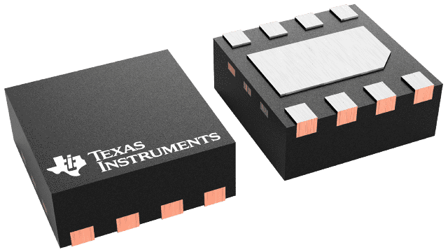
- Package
- WSON-8
Product overview
The BQ2947 is a second-level overvoltage protector for 2-, 3- or 4-series cell Li-ion battery packs, monitoring each cell and triggering an external FET off-state when any cell exceeds its overvoltage threshold (selectable from 4.125 V to 4.6 V). It uses a single-pin output drive with an external delay capacitor to set the fault response time and consumes only 1 uA typical operating current. It is intended as a backup protection device used alongside a primary battery management IC.
- Manufacturer
- TI
- Part number
- BQ294704DSGT
- Category
- Battery Management
- Package
- WSON-8
- Packaging
- Tape & Reel
- Condition
- New & Original
- Compliance
- RoHS Compliant
- Lifecycle
- Confirm with manufacturer
- Lead time / MOQ
- Confirm with quotation
Technical parameters
34 parametersConstruction
- BQ294700, RIN = 1kΩ
- 4 V
- BQ294701, RIN = 1kΩ
- 4 V
- BQ294702, RIN = 1kΩ
- 4 V
- BQ294703, RIN = 1kΩ
- 4 V
- BQ294704, RIN = 1kΩ
- 4 V
- BQ294705, RIN = 1kΩ
- 4 V
- VOV BQ294706, RIN = 1kΩ
- 4 V
- BQ294707, RIN = 1kΩ
- 4 V
- BQ294708, RIN = 1kΩ
- 4 V
- BQ294711, RIN = 1kΩ
- 4 V
- BQ294712, RIN = 1kΩ
- 4 V
- BQ294713, RIN = 1kΩ
- 4 V
- BQ294715, RIN = 1kΩ
- 3 V
- VHYS OV Detection Hysteresis BQ2947
- 300 mV
- VOA OV Detection Accuracy TA = 25°C
- 10 mV
- OV Detection Accuracy TA = 0°C
- 20 mV
- ICELL
- 1.1 µA
- VDD = 14.4V, IOL = 100 µA measured into
- 250 mV
- IOUTH = 14.4V
- 4. 5mA
- IOUTL
- 14 mA
- VOUT VDD = 14.4V, IOL = 100 µA measured into
- 250 mV
- IOUTLK OUT pin leakage VDD = 14.4V
- 100 nA
- tCD_GND
- 170 ms
Performance
- Supply voltage VDD–VSS
- 30 V
- Input voltage V4V3, V3V2, V2V1, V1–VSS, or CD–VSS
- 30 V
- Output voltage OUT–VSS
- 30 V
- Lead temperature (soldering, 10s)
- 300
- Storage temperature, Tstg
- 150
- Supply voltage
- 20 V
- Input voltage range V4V3, V3V2, V2V1, V1–VSS, or CD–VSS
- 5 V
- Operating ambient temperature range
- 110 °C
- Across Temperature TA = 60°C
- 24 mV
- IDD Supply Current
- 1 2µA
- IIN Input Current at Vx Pins
- 0. 1µA
Specifications & documentation
Use the official manufacturer documentation to verify electrical characteristics, package dimensions and operating limits before design approval.
Request confirmation of current stock, date code, packaging, price and delivery terms. Product information does not constitute a binding offer; final specifications are confirmed with your quotation.