
BQ25892RTWR
The BQ25892 is an I2C-controlled single-cell 5-A switch-mode buck battery charger with an NVDC power path, supporting 3.9 V to 14 V input and adjustable USB On-The-Go boost mode. It integrates an ADC, input-current optimization (ICO), input-current limit, input OVP, JEITA thermistor monitoring and IC thermal regulation. Typical use is fast charging of single-cell Li-Ion/Li-Polymer packs in mobile and portable applications over an -40 to 85 C range.
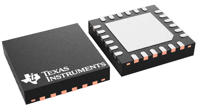
- Package
- WQFN-24
Product overview
The BQ25892 is an I2C-controlled single-cell 5-A switch-mode buck battery charger with an NVDC power path, supporting 3.9 V to 14 V input and adjustable USB On-The-Go boost mode. It integrates an ADC, input-current optimization (ICO), input-current limit, input OVP, JEITA thermistor monitoring and IC thermal regulation. Typical use is fast charging of single-cell Li-Ion/Li-Polymer packs in mobile and portable applications over an -40 to 85 C range.
- Manufacturer
- TI
- Part number
- BQ25892RTWR
- Category
- Battery Management
- Package
- WQFN-24
- Packaging
- Tape & Reel
- Condition
- New & Original
- Compliance
- RoHS & REACH Compliant
- Lifecycle
- Confirm with manufacturer
- Lead time / MOQ
- Confirm with quotation
Technical parameters
38 parametersConstruction
- LSFET. Connect the
- 0.047µF bootstrap cap
- VBUS (converter not switching)
- 22
- PMID (converter not switching)
- 22
- STAT
- 20
- PG (BQ25892)
- 7
- DSEL (BQ25890)
- 20
- BTST
- 20
- SW
- 16
- BAT, SYS (converter not switching)
- 6
- SDA, SCL, INT, OTG, REGN, TS, CE
- 7
- PSEL (BQ25892)
- 7
- D+, D– (BQ25890)
- 7
- BTST TO
- 7
- PGND to
- 0.3
- ILIM
- 5
- INT
- 6
- Human body model (HBM), per ANSI/ESDA/JEDEC JS-001
- ±2000 V
- (REG09[5]=1), battery monitor disabled, TJ <
- 12 µA
- (REG09[5]=0), battery monitor disabled, TJ <
- 32 µA
- (REG09[5]=1)
- 50 mV
- (REG03[3:1]=10
- 1), ISYS
- VBAT = 4.35 V
- = 3.5V
- VBUS and PMID TJ = –40°C to +12
- 5°C
- and SW T = –40°C to +125°
- 27
- SW and GND TJ = –40°C to
- +125°C
Performance
- Output sink current PG (BQ25892)
- 6
- Junction temperature
- 150
- Storage temperature range, Tstg
- 150
- VIN Input voltage
- 14(1) V
- IIN Input current (VBUS)
- 3.25 A
- ISYS Output current (SW)
- 5 A
- VBAT Battery voltage
- 4.608 V
- Fast charging current
- 5 A
- Discharging current with internal
- 9 (pe
- TA Operating free-air temperature range
- 85 °C
- I(BADSRC) Bad adapter detection current source
- 30
- VSYS(MIN) Minimum DC system voltage output
- 3.50
- VSYS(MAX) Maximum DC system voltage output
- 4.40
Specifications & documentation
Use the official manufacturer documentation to verify electrical characteristics, package dimensions and operating limits before design approval.
Request confirmation of current stock, date code, packaging, price and delivery terms. Product information does not constitute a binding offer; final specifications are confirmed with your quotation.