
ADC108S102CIMTX/NOPB
The ADC108S102 is an 8-input, 10-bit successive-approximation (SAR) ADC supporting sample rates from 500 kSPS to 1 MSPS with a single 2.7-V to 5.25-V supply. It uses a SPI/Microwire-compatible serial interface, consumes about 2.1 mW typical, and operates from -40°C to +105°C. It is used in sensor and data-acquisition systems requiring multiple single-ended input channels.
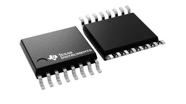
- Package
- TSSOP-16
Product overview
The ADC108S102 is an 8-input, 10-bit successive-approximation (SAR) ADC supporting sample rates from 500 kSPS to 1 MSPS with a single 2.7-V to 5.25-V supply. It uses a SPI/Microwire-compatible serial interface, consumes about 2.1 mW typical, and operates from -40°C to +105°C. It is used in sensor and data-acquisition systems requiring multiple single-ended input channels.
- Manufacturer
- TI
- Part number
- ADC108S102CIMTX/NOPB
- Category
- Data Converters
- Package
- TSSOP-16
- Packaging
- Tape & Reel
- Condition
- New & Original
- Compliance
- RoHS Compliant
- Lifecycle
- Confirm with manufacturer
- Lead time / MOQ
- Confirm with quotation
Technical parameters
37 parametersConstruction
- Resolution with No Missing Codes
- 10 Bits
- INL
- ±0.2 B(max)
- DNL Differential Non-Linearity
- ±0.2 B(max)
- VOFF Offset Error
- +0.3 B(max)
- OEM Offset Error Match
- ±0.07 B(max)
- FSE Full Scale Error
- +0.2 B(max)
- FSEM Full Scale Error Match
- ±0.07 B(max)
- FPBW Full Power Bandwidth (−3dB)
- 8 MHz
- SNR Signal-to-Noise Ratio fIN = 40.2 kHz, −0.02 dBFS
- 61.8 B(min)
- THD Total Harmonic Distortion fIN = 40.2 kHz, −0.02 dBFS
- −87.0 (max)
- SFDR Spurious-Free Dynamic Range fIN = 40.2 kHz, −0.02 dBFS
- 83.1 B(min)
- ENOB Effective Number of Bits fIN = 40.2 kHz
- 9.98 ts(min)
- ISO Channel-to-Channel Isolation fIN = 20 kHz
- 79.7 dB
- fa = 19.5 kHz, fb = 20.5 kHz
- −83.9 dB
- VIN Input Range
- 0 to VA V
- Track Mode
- 33 pF
- Hold Mode
- 3 pF
- VA = VD = +2.7V to +3.6V
- 2.1 (min)
- VA = VD = +4.75V to +5.25V
- 2.4 (min)
- CIND Digital Input Capacitance
- 2 (max)
- COUT Hi-Impedance Output Capacitance
- 2 (max)
- tCSH CS Hold Time after SCLK Rising Edge
- 0 s(min)
- tCSS
- 5 s(min)
- tEN CS Falling Edge to DOUT enabled
- 5 (max)
- tDACC
- 17 (max)
- tDHLD
- 4 s(typ)
- tDS
- 3 s(min)
- tDH DIN Hold Time after SCLK Rising Edge
- 3 s(min)
- tCH SCLK High Time
- 0.4 x tSCLK s(min)
- tCL SCLK Low Time
- 0.4 x tSCLK s(min)
- CS Rising Edge to DOUT High- DOUT falling
- 2.4 (max)
- Impedance DOUT rising
- 0.9 (max)
Performance
- IDCL DC Leakage Current
- ±1 (max)
- VIL Input Low Voltage VA = VD = +2.7V to +5.25V
- 0.8 (max)
- IIN Input Current VIN = 0V or
- ±0.01 (max)
- VOL Output Low Voltage ISINK = 200 µA to 1.0 mA
- 0.4 (max)
- IOZH, IOZL Hi-Impedance Output Leakage Current
- ±1 (max)
Specifications & documentation
Use the official manufacturer documentation to verify electrical characteristics, package dimensions and operating limits before design approval.
Request confirmation of current stock, date code, packaging, price and delivery terms. Product information does not constitute a binding offer; final specifications are confirmed with your quotation.